MoS2 Transistor Study Reports 85% Less Contact Variability — in Simulation
A*STAR reports simulations of recessed Ti contacts on MoS₂ with lower barrier variability. We distinguish the modelling evidence from fabricated devices.
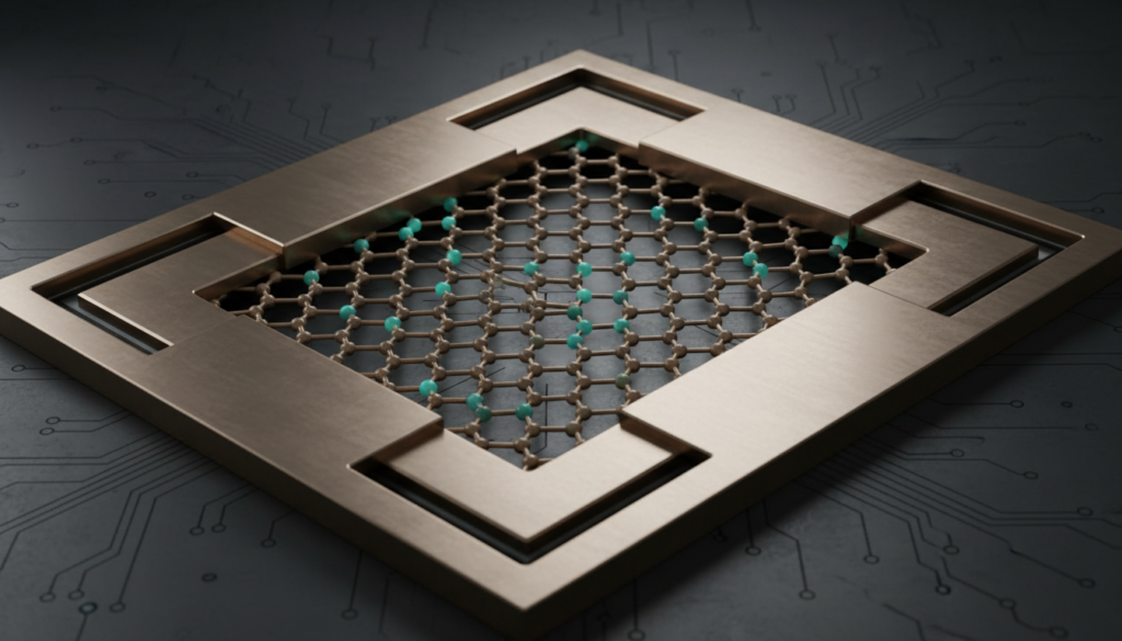
Original DeepTech conceptual illustration. Not a microscopy image, fabricated device or computational output from the MoS₂ study.
An atomic-scale transistor research study has identified a potential way to reduce sensitivity to defects in next-generation semiconductor materials. Scientists at Singapore’s A*STAR compared two arrangements for metal contacts on molybdenum disulfide (MoS₂) and reported that one contact design reduced modelled variations in an electrical injection barrier by approximately 85%. The paper appeared in npj 2D Materials and Applications on 6 November 2026. Its findings are based on electronic-structure and transport simulations, not measurements on newly fabricated commercial chips.
The authors, Hangbo Zhou, ZhiGen Yu and Yong-Wei Zhang, published a peer-reviewed journal article and provided computational materials through a public Materials Cloud dataset. Those records allow examination of the specific models behind the headline. They do not independently validate industrial manufacturing yield or transistor lifetime.
Image disclosure: the featured illustration is original conceptual DeepTech artwork of a MoS₂ sheet and metallic contacts, not an experimental micrograph or actual simulation output.
Why transistor contacts can limit new semiconductors
A field-effect transistor moves electrical carriers through a semiconductor channel between metal contacts. The quality of the interface at which the carriers enter the channel can be as important as the material inside it. Resistance and energy barriers at this interface can prevent a device from realizing the performance suggested by the semiconductor’s intrinsic properties.
MoS₂ is a widely studied two-dimensional semiconductor because its channels can be atomically thin. Yet lattice imperfections can affect how current passes from metal into the layer. Missing sulfur atoms, known as sulfur vacancies, are particularly relevant. If contact behavior changes substantially depending on where such a vacancy sits, nominally similar devices could differ in their electrical behavior.
What geometries did the team compare?
The research uses matched theoretical models of a conventional one-sided titanium contact and a double-sided recessed contact geometry. The researchers applied a comparable ordered set of sulfur-vacancy locations to each model. This controlled design makes it easier to isolate the effect of the metal contact arrangement from changes in the particular defects being studied.
Calculations of electron structure and non-equilibrium transport provide estimates of interface barriers and electron transmission. These are valuable tools for generating device-design hypotheses, but their output is contingent on model assumptions and numerical parameters. They cannot establish how consistently a complex physical contact will be produced in a semiconductor fabrication line.
What the study found about barrier height
For a specified near-edge vacancy in the studied structures, the paper reports a Schottky barrier height of 0.58 eV in the one-sided top-contact model and 0.21 eV in the double-sided recessed model. A lower barrier can help electrical carriers cross an interface. That relationship alone does not determine total device performance, which also depends on channel properties and operational conditions.
Across the specified sequence of vacancy positions, the authors report a reduction of approximately 85% in nominal barrier-height variation for the recessed configuration. This number is a sensitivity result within their comparative simulations. It is not an 85% reduction in power consumption, a manufacturing-yield improvement or a measured speed increase for a working processor.
Why transport modelling adds context
The study also compares calculated electron transmission, reporting improved transmission and lower access energies for propagating channel states in the recessed contact arrangement. Those results are consistent with the idea that the contact geometry may make carrier injection more tolerant of defect positioning.
The next engineering challenge is translating such a geometry into practical devices. Forming contacts around an atomically thin semiconductor could impose fabrication constraints, introduce other defects or complicate integration. The models do not resolve these possibilities, and they do not establish reliability after many operating cycles.
How auditable are the simulations?
The Materials Cloud archive includes atomic structures, calculation inputs and metadata relating to vacancy coordinates, contact geometry, convergence and barrier extraction. This is useful because it allows independent investigators to inspect details that are often missing from a press summary. A reproducibility exercise would still need compatible software and computational settings, and should explicitly track any differences from the original results.
A separate physical study would be necessary to determine if the modelled reductions actually occur in manufactured samples. The value of open research artifacts is traceability, not an automatic certification that every implied application has been proven.
Where this fits into semiconductor development
The industry is studying new channel materials and three-dimensional architectures as conventional scaling faces complex constraints. Contact resistance, thermal issues and fabrication control all matter alongside transistor dimensions. This A*STAR work focuses on a narrow but meaningful part of that broader research: how a contact responds to atomic defects in a two-dimensional channel.
It is distinct from IBM’s separate nanostack initiative, which we covered in our analysis of emerging 3D transistor manufacturing. Similar industry goals do not mean that the underlying experiments or maturity levels are interchangeable.
What independent validation should follow?
The decisive next step is to manufacture comparable one-sided and recessed-contact MoS₂ devices, measure the relevant barriers and resistances repeatedly, and report the full spread of observed outcomes. Device reliability, yield, interface quality and the influence of actual defect distributions should be included. The same tests should be reproduced outside the original simulation team.
That transition from well-documented computational evidence to practical manufacturing is one of the barriers discussed in our guide to deep-tech adoption. The present paper supports a design hypothesis and a quantitative model comparison. It does not establish an industrially qualified transistor.
A bounded research conclusion
A*STAR’s theoretical results indicate that a recessed double-sided titanium contact may stabilize carrier injection when sulfur-vacancy locations vary in modeled MoS₂ systems. The change from 0.58 to 0.21 eV in one barrier example and the approximately 85% reduction in positional variation are meaningful within those calculations. They remain computational findings; further experimental fabrication and independent measurement are needed before any commercial device claims are justified.