IBM Siemens Nanostack: The Road From 3D Transistors to Manufacturable Chips
IBM and Siemens are collaborating on 3D nanostack transistor research. The announcement centers on design and manufacturing challenges, not mass production.
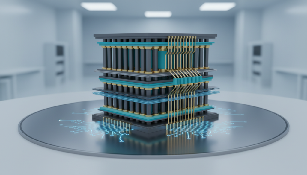
Original conceptual illustration for DeepTech; not a documentary photograph or screenshot.
The IBM Siemens nanostack collaboration points to a problem at the heart of advanced semiconductors: demonstrating a novel transistor structure is not the same as manufacturing millions of chips at acceptable cost and yield. On 14 October 2026, IBM and Siemens announced research involving new design and simulation methods for IBM’s three-dimensional nanosheet transistor architecture. The partnership is focused on making future generations easier to design and build—not announcing that nanostack processors have entered mass production.
What is the nanostack research about?
Conventional chip improvement is often explained through smaller features on a flat surface. IBM’s nanostack concept instead places nanosheet-based transistors in vertical and staggered arrangements. The aim is to put more transistor structures into a given area while retaining options to optimize individual layers. IBM says it previously demonstrated a 7-angstrom-node implementation of its research concept.
In the company’s description, the demonstrated structure approaches 100 billion transistors in an area comparable to a fingernail. This is a company-reported research claim, not a specification for a commercially available laptop or data-center processor. Also, the 7-angstrom name refers to an industry technology-node designation; it should not be read as a promise that every physical feature measures exactly seven angstroms.
Why is Siemens involved in IBM’s 3D transistor work?
A sophisticated transistor architecture needs much more than a clever cross-section. Engineers must model behavior, design layouts, simulate manufacturing processes, tune lithography and determine which combinations can be reproduced across wafers. Siemens brings expertise in electronic design automation and manufacturing software, while IBM brings device research and fabrication knowledge.
The announced plan includes virtual models intended to explore performance and fabrication difficulties before physical chips are built. Computer simulation can reduce expensive iterations, but it cannot replace experimental manufacturing evidence. Defects, materials compatibility, heat dissipation, electrical variability and production yield still have to be addressed in reality.
Does a 3D stack automatically make chips faster or greener?
No. Higher theoretical density can support new architectural options, but operating power, heat, switching performance and usable output depend on design choices and manufacturing outcomes. A headline about transistor count does not specify the energy consumed by a finished processor on an actual workload. Performance and efficiency claims need a clearly identified test setup and comparable chips.
A separate IBM announcement from June 2026 described the earlier nanostack demonstration. October’s announcement adds a development collaboration rather than a second commercially deployed chip. Keeping these milestones separate prevents a research partnership from being mistaken for a product launch.
How can readers judge the next milestone?
The most informative progress would include independently reproducible measurements on fabricated devices, working circuits rather than isolated samples, quantified yield across wafers and reliable lifetime data. Later, third-party benchmarks could assess throughput and energy consumption in complete systems. Until these data are available, the strongest defensible claim is that IBM and Siemens are working on the tools needed to move from device research toward manufacturability.
For wider context on translating research into industrial scale, see DeepTech’s overview of nanotechnology manufacturing barriers.
Why the collaboration matters
Advanced computing has large economic and energy implications, but breakthroughs can stall between a laboratory demonstration and commercial volume. The willingness to invest in design automation and process models signals that manufacturability is a central part of the challenge. Whether nanostack ultimately changes the mainstream chip industry will depend on evidence from fabrication and adoption rather than on a press-release label.
Primary sources
• IBM — nanostack research collaboration with Siemens, 14 October 2026.
• IBM — earlier nanostack research demonstration, 25 June 2026.
Editorial note: Reported density and technology-node claims come from IBM. This article does not assert commercial availability or independent reproduction. Featured image is a conceptual illustration.